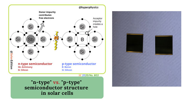
In most cases, the thickness of the p-layer is greater than that of the n-layer because the p-type substrate absorbs the most sunlight. The n-type layer should be very thin because its main function is to transmit solar radiation to the p-type layer.
The p-type is doped with beryllium, the n-type is doped with tellurium, GaAs is a group III-V compound semiconductor, beryllium is a group II element, and the replacement gallium ionizes to form holes, and tellurium is a group VI element, and the replacement arsenic ionizes to form electrons.

The side that the light illuminates first is critical; for the sake of illustration, assume it is the n-side. Since the n-type is the first surface irradiated by light, it is particularly important to effectively capture electron-hole pairs. If it is too long, then it is too long on the surface, the point furthest from the junction, the point with the strongest absorption (absorption decreases exponentially from the surface).
Gallium arsenide (GaAs) is one of the important materials for terahertz-band semiconductor heterostructure lasers. In order to obtain the optical properties of p-type GaAs materials in the far-infrared band, gaseous source molecular beam epitaxy (GSMBE) technology is used in semi-insulating GaAs ( 100) Be-doped p-type GaAs thin film materials are grown on the substrate, and the carrier concentration ranges from 1.54×10¹⁵ to 1.85×1019 cm-3. The far-infrared reflectance spectrum is measured with a far-infrared transform Fourier spectrometer, and the The reflection spectrum has been simulated and analyzed theoretically, and the refractive index, extinction coefficient and absorption coefficient of p-type GaAs with different hole concentrations in the far-infrared band are calculated. It is found that the extinction coefficient and absorption coefficient in this band are all with the current-carrying The increase of the sub-concentration increases, and the maximum absorption coefficient can reach 4.0×104cm-1.