Development and utilization of gallium arsenide electronic devices according to the high electron mobility of gallium arsenide, it is an ideal device material for developing ultra-high speed computers. Its electron mobility is about 5 times higher than that of silicon, and its computing speed is much higher than that of silicon devices. In the 1970s and 1980s, people predicted and valued it one after another.
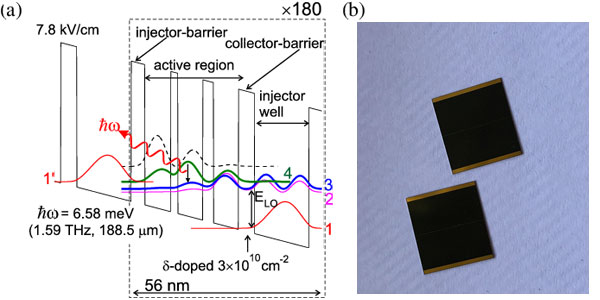
Active region of GaAs optoelectronic devices application of GaAs optoelectronic devices: visible light emitting diodes. Because of its small size, energy saving, fast response and long service life, it is widely used in household appliances, office equipment, billboards, traffic lights and automobile tail lights; Infrared LED. Used as remote control, optical isolator, etc.

Gallium arsenide is a compound semiconductor material with the molecular formula GaAs. Cubic zinc blende structure, that is, a compound lattice composed of face centered cubic lattice composed of as and Ga atoms, with a lattice constant of 5.6419a. At room temperature, the band gap is 1.428ev. It is a direct band gap semiconductor with a melting point of 1238 ℃, a mass density of 5.307g/cm3 and a permittivity of 13.18. The conduction band of GaAs single crystal is a double energy valley structure. Its lowest energy valley is located in the center of the first Brillouin region, and the electron effective mass is 0.068m0 (M0 is the electron mass, see carrier). The second lowest energy valley is located at point L in the < 111 > direction, which is about 0.29ev higher than the lowest energy valley, its electron effective mass is 0.55m0, and the valence band top is about located in the center of the Brillouin region, The effective masses of light holes and heavy holes in the valence band are 0.082m0 and 0.45m0, respectively. The electron and hole mobility of pure GaAs crystals are 8000 cm2 / (V· s) and 100 ~ 300 cm2 / (V · s), respectively, and the minority carrier lifetime is 10-2 ~ 10-3 μ s。 N-type semiconductors can be obtained by doping Group VI elements te, Se, s or group IV Elements Si. P-type semiconductors can be prepared by doping group II elements be and Zn. Semi insulating materials with resistivity up to 107 ~ 108 Ω· cm can be made by doping CR or improving purity. In recent ten years, due to the development of molecular beam epitaxy and metal organic chemical vapor deposition (MOCVD) technology, heterojunctions and superlattices can be prepared on GaAs single crystal substrates. These structures have been used to make new semiconductor devices, such as high electron mobility transistor (HEMT), heterojunction bipolar transistor (HBT) and laser, which has developed a broader prospect for the application of GaAs materials.