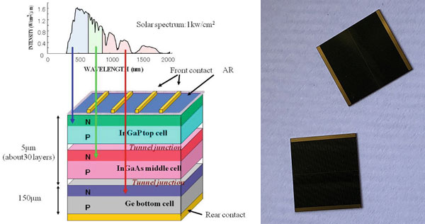
How are gaas solar cells made, Its similar to silicon, gallium arsenide materials can also be divided into bulk single crystal and epitaxial materials. Bulk single crystals can be used as substrate materials for epitaxy, or integrated circuits can be directly manufactured using ion implantation doping processes (using high-quality, large cross-section, semi-insulating gallium arsenide single crystals). The focus is on the liquid-sealed Czochralski method (ie, the liquid-sealed Chochrassky method, or LEC method for short), but the horizontal boat growth method (ie, the horizontal Bridgman method) produces a single crystal with better quality and uniformity. Still received a certain amount of attention. A new development of the liquid-sealed Czochralski method is to use pyrolytic boron nitride (PBN) crucible and dry boron oxide liquid sealing agent to directly synthesize and pull undoped, semi-insulating gallium arsenide single crystals in a high-pressure single crystal furnace . In addition, the method of using quartz crucible and water-containing boron oxide as the liquid sealing agent under normal pressure has also been successfully tested. Regardless of the horizontal boat growth method or the liquid-sealed Czochralski method, the diameter of the crystal can reach 100-150 mm, which is similar to that of a silicon single crystal.

The epitaxial growth of gallium arsenide can be divided into gas phase and liquid phase epitaxy according to the process, and the obtained epitaxial layer is superior to bulk single crystal materials in terms of purity and crystal integrity. The general gas phase epitaxy process is the Ga/AsCl3/H2 method, and alternative processes of this method are Ga/HCl/AsH3/H2 and Ga/AsCl3/N2 methods. In order to improve the quality of the gas phase epitaxial layer of the Ga/AsCl3/H2 system, the epitaxial growth process at low temperature and low temperature and low pressure has also been studied. The liquid phase epitaxy process is to cover the surface of the substrate with a Ga/GaAs molten pool, and then grow the epitaxial layer by cooling down. Temperature gradient growth or electric epitaxy with direct current can also be used. In the manufacture of devices (especially microwave devices), vapor phase epitaxy is more widely used than liquid phase epitaxy. Liquid phase epitaxy can be used to manufacture heterojunctions (such as GaAs/AlxGa1-xAs), so it is an important method for manufacturing gallium arsenide double heterojunction lasers and solar cells.