Semiconductor heterojunction is a special PN junction, which is formed by depositing more than two layers of different semiconductor material films on the same base. These materials have different energy band gaps. They can be compounds such as gallium arsenide or semiconductor alloys such as silicon germanium.
Heterojunction, the interface region formed by the contact of two different semiconductors. According to the different conductive types of the two materials, heterojunctions can be divided into homogeneous heterojunctions (P-P junction or N-N junction) and heterogeneous heterojunctions (p-n or p-n). Multilayer heterojunctions are called heterostructures. The general conditions for the formation of heterojunction are that the two semiconductors have similar crystal structure, similar atomic spacing and thermal expansion coefficient. Heterojunctions can be fabricated by using interface alloy, epitaxial growth, vacuum deposition and other technologies. Heterojunction often has excellent photoelectric characteristics that neither PN junction of two semiconductors can achieve, which makes it suitable for making ultra-high speed switching devices, solar cells and semiconductor lasers.
The middle layer or the interlayer on both sides of the semiconductor heterostructure can be changed according to different needs. For example, in the case of gallium arsenide, gallium can be replaced by aluminum or indium, while arsenic can be replaced by phosphorus, antimony, or nitrogen. Therefore, the designed material properties vary. Therefore, the term "artificial material engineering" appears. Recently, scientists have found ferromagnetism by replacing gallium with manganese atoms, which has attracted great attention, because future semiconductor components may use the characteristics of electron spin. In addition, in semiconductor heterostructures, if the atomic spacing between the adjacent two layers is different, the arrangement of atoms will be forced to be the same as that of the lower layer, then there will be stress between atoms, which will change the energy band structure and behavior of electrons. Now the magnitude of this stress can be controlled by long crystal technology, so scientists have another factor to adjust semiconductor materials to produce more novel components, such as silicon germanium heterostructure high-speed transistors.
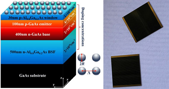
The density of interface states can significantly affect the carrier recombination at the heterojunction interface between graphene and GaAs and the corresponding photovoltaic properties. In addition, the work function of the back electrode has a significant impact on carrier transmission and collection. Therefore, the work function of the back electrode should also be considered when selecting the back electrode material. In addition, when the alxga1 XAS (x = 0.2) buffer layer is introduced into the heterojunction interface, an enhanced photovoltaic conversion efficiency of 24.78% can be achieved. Finally, the comparison between the simulation and experimental data of graphene / GaAs Heterojunction Solar cells is introduced. This study shows that graphene / GaAs Heterojunction has great application potential in high efficiency solar cells.