Fabricating of gallium arsenide:
Similar to silicon, gallium arsenide can be divided into bulk single crystal and epitaxial materials. Bulk single crystal can be used as substrate material for epitaxy, and can also be directly used to fabricate integrated circuits by ion implantation doping process. The key point is the liquid sealed Czochralski method (LEC Method), but the horizontal boat growth method (horizontal Bridgman method) is still paid attention to because of its good quality and uniformity. A new development of liquid sealed Czochralski method is the direct synthesis and drawing of undoped, semi insulating GaAs single crystals in a high pressure single crystal furnace using pyrolytic boron nitride (PBN) crucible and dry boron oxide liquid sealing agent. In addition, the method of using quartz crucible and hydrous boron oxide as liquid sealing agent under normal pressure has also been successfully tested. Whether the horizontal boat growth method or the liquid sealed Czochralski method, the diameter of the crystal can reach 100-150 mm, which is similar to that of single crystal silicon.

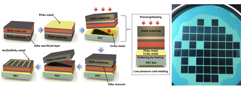
The epitaxial growth of GaAs can be divided into vapor phase epitaxy and liquid phase epitaxy. The purity and crystal integrity of the epitaxial layer obtained are better than that of bulk single crystal materials. The general vapor phase epitaxy process is GA / ascl3 / H2 method, and the alternative processes are GA / HCl / AsH3 / H2 and GA / ascl3 / N2 methods. In order to improve the quality of gas phase epitaxial layer in GA / ascl3 / H2 system, epitaxial growth processes at low temperature and low pressure were also studied. Liquid phase epitaxy (LPE) is a process in which the substrate surface is covered with GA / GaAs molten pool, and then the epitaxial layer is grown by cooling down. It can also be grown by temperature gradient method or by applying direct current. Vapor phase epitaxy is more widely used than liquid phase epitaxy in the manufacture of devices (especially microwave devices). Liquid phase epitaxy (LPE) can be used to fabricate heterojunction (such as GaAs / alxga1 XAS), so it is an important method to fabricate GaAs double heterojunction lasers and gaas solar cells.
GaAs devices mainly include optoelectronic devices and microwave devices. Gallium arsenide and other Ⅲ - Ⅴ compounds have direct transition band structure, and are in a favorable position in photoelectric applications. Commonly used optoelectronic devices include alxgaas / GaAs and ingaxpasy / InP double heterojunction lasers, infrared and visible light emitting diodes, and GaAs solar cells.