The gallium, arsenic source or their derivatives are deposited by vapor deposition or liquid deposition,Gallium arsenide or other material is a single crystal thin of gallium arsenide or other material grown on the surface of the substrate,Films are collectively referred to as gallium arsenide epitaxial materials. If the substrate and epitaxial layer are composed of the same material, It is called homogeneous junction epitaxial layer. If it is composed of different materials, it is called heterojunction epitaxial layer. Epitaxial material
The material can be a single-layer structure or a multi-layer structure. The preparation methods of epitaxial materials mainly include Vapor phase epitaxy and liquid phase epitaxy. With the progress of technology and the expansion of application, in order to adapt to the relaxation of the ban to meet the needs of device manufacturing such as band, multicomponent compound, quantum well and superlattice structure and the development of new technologies such as metal organic vapor deposition and molecular beam epitaxy have developed rapidly.

Vapor phase epitaxy: a method of thin film growth through gas phase transport and gas phase reaction.Process. GaAs epitaxial layers are usually grown by chloride method and hydride method,Ga-asc13-h2 has become a representative process of chloride method, which is characterized by easy realization of high purity raw material.
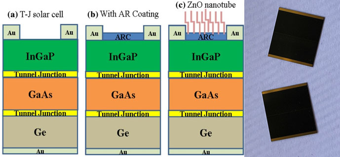
X-ray diffraction shows that the crystal structure of the sample in the vertical surface direction is ZnO nanotube structure,Hall measurement shows that the electrical properties of the sample before annealing belong to n-type semiconductor. When annealing at 600 ° C, the electrical properties of zinc oxide will be converted from n-type to p-type semiconductor. This is mainly because arsenic and gallium diffuse into hydrothermal-deposited ZnO nanotube structure.The optical properties of the sample are measured by fluorescence spectrum. From the fluorescence spectrum, it can be known that the change of the position of energy gap luminescence implies the change of electrical properties. From X-ray photoelectron spectroscopy and energy dispersion analyzer, it can be known that arsenic and zinc bonds will provide holes in electrical properties, which is due to the formation of complexes when gallium is mixed into zinc oxide films, which can explain the change in electrical properties.