Generally speaking, the high-efficiency multi junction solar cell refers to the solar spectrum, selecting semiconductor materials with different bandwidth in different bands to make multiple solar sub cells, and finally connecting these sub cells in series to form multi junction solar cells.
At present, the conversion efficiency of more studied III-V material systems, such as InGaP / GaAs / Ge triple junction cell, can reach about 42.8%. II-VI materials are also selected, but they are still in the research stage. This paper will mainly introduce InGaP / GaAs / Ge and other III-V material systems.The theoretical efficiency of single junction GaAs cell is 30%.Since the 1980s, GaAs solar cell technology has experienced several development stages from LPE to MOCVD, from homogeneous epitaxy to heterogeneous epitaxy, and from single junction to multi junction laminated structure. Its development speed has been accelerated and its efficiency has been continuously improved. At present, the maximum efficiency of the laboratory has reached 50% (data from IBM), and the industrial production conversion rate can reach more than 30%.
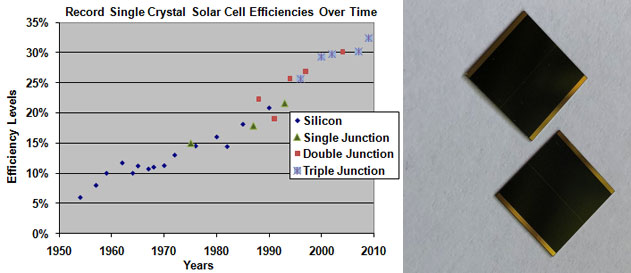
The band gap of GaAs is wider than that of silicon, which makes its spectral response and space solar spectral matching ability better than that of silicon. The theoretical efficiency of single junction GaAs cell is 30%, while that of multi junction GaAs cell is more than 50%. In general, the temperature resistance of gallium arsenide cell is better than that of silicon photocell. Experimental data show that gallium arsenide cell can still work normally at 250 ℃, but silicon photocell can not work normally at 200 ℃. Gallium arsenide is more brittle than silicon in physical properties, which makes it easier to crack during processing. Therefore, it is often made into thin films and substrates (often Ge [germanium]) are used to combat its disadvantages in this regard, but it also increases the complexity of the technology. The development of GaAs solar cells began in the 1950s and has a history of more than 50 years. In 1954, GaAs Materials with photovoltaic effect were found for the first time in the world. In 1956, loferski J.J. and his team discussed the physical properties of the best materials for manufacturing solar cells. They pointed out that the materials with eg in the range of 1.2 ~ 1.6ev have the highest conversion efficiency. (eg of GaAs material is 1.43ev. In the above high efficiency range, it is theoretically estimated that the efficiency of GaAs single junction solar cell can reach 27%). In the 1960s, gobat and others developed the first zinc doped GaAs solar cell, but the conversion rate was not high, only 9% ~ 10%, far lower than the theoretical value of 27%. Since the 1980s, GaAs solar cell technology has experienced several development stages from LPE to MOCVD, from homogeneous epitaxy to heterogeneous epitaxy, and from single junction to multi junction laminated structure. Its development speed has been accelerated and its efficiency has been continuously improved.