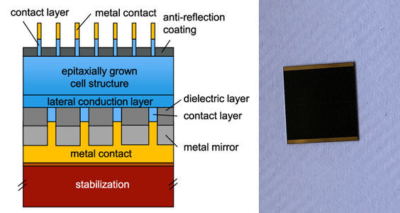
One possibility to reduce the radiation recombination loss and therefore increase the open circuit voltage of GaAs single junction solar cells is to enhance photon recovery. Generally speaking, photon emission occurs in semiconductors at all solid angles, and the absolute probability of radiation recombination increases with the increase of crystal quality. The possibility of the emitted photons being reabsorbed is very low, so it is important to ensure a long enough path. This is achieved by repeatedly reflecting light between the front and rear of the solar cell structure. On the front, the exit cone is determined by the high refractive index step from GaAs to air, resulting in an exit cone of about 16 °, which is not affected by the additional planar antireflective coating. For greater than critical angle(θc).Total internal reflection will occur.

However, on the back, photons emitted at all angles are usually transmitted to the GaAs substrate, where parasitic absorption occurs. One possibility to reduce this loss is to replace the substrate with a mirror. According to the simulation, VOC increases superlinearly with the increase of mirror reflectivity. This increase is particularly evident for reflectance above 95%. Therefore, it is very important to provide a mirror with high reflectivity to benefit from nonlinear voltage rise.
The reflectivity of metal mirrors is usually limited. However, the loss can be reduced by introducing an additional dielectric layer between the photoactive GaAs cell and the metal mirror. In this concept, total internal reflection occurs at the semiconductor dielectric interface for all photons greater than the critical angle. In addition, photons transmitted through the dielectric layer have a second chance to be reflected in the metal mirror. Since the proportion of photons reaching the metal mirror is small, the parasitic absorption loss at the metal is reduced. Of course, these losses are also highly dependent on the type of metal. This method is similar to passivating emitter and back cell silicon solar cells. Dielectric metal stacks are also used in LED devices to improve external coupling efficiency.
We use silver as a metal because it has high reflectivity in the relevant wavelength range of GaAs emission, and magnesium fluoride as a dielectric coating. MgF2 has a low refractive index in the range of 1.38-1.42, resulting in a large amount of total internal reflection. Any other dielectric with low refractive index will also be suitable.